C & L Impedance
Capacitor Impedance
ZC=jωC1=−ωCj
Inductor Impedance
ZL=jωL
Amplifiers
I will generalize all single stage operational amplifiers using the following two-input system.

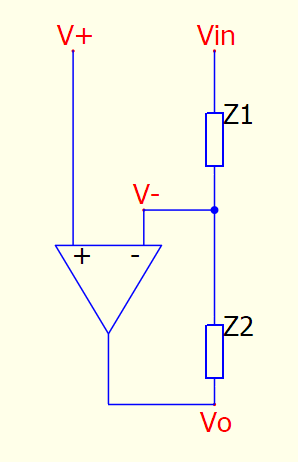
The basic function of an op-amp is to ensure V+=V−. In terms of feedback systems, you can think of the output Vo as the control signal meant to steer V− towards V+ to minimize error, while Vin is a disturbance signal. For the following examples, we assume infinite input impedance (no current flowing into our inputs) and zero output impedance. With these assumptions, we get the following:
V−=Z1+Z2Z2(Vin+Vo)+Vo
=Z1+Z2Z2Vin+(1−Z1+Z2Z2)Vo
=Z1+Z2Z2Vin+Z1+Z2Z1Vo
Then, using using V+=V−, we have the following equation:
V+=Z1+Z2Z2Vin+Z1+Z2Z1Vo
Z1+Z2Z1Vo=V+−Z1+Z2Z2Vin
Vo=(Z3Z1+Z2)V+−(Z1Z1+Z2)(Z1+Z2Z2)Vin
=Z1Z1+Z2V++−Z1Z2Vin
For a basic inverting amplifier, let us ground our non-inverting input, V+=0V. Then, using the above equations, we get:
Vo=−Z1Z2Vin
Giving us a voltage-gain of VinVo=−Z1Z2
For a basic non-inverting amplifier, let us consider the input to be V+ and ground Vin. Now, we have
Vo=Z1Z1+Z2V+
Giving us a voltage-gain of V+Vo=Z1Z1+Z2
The usefulness of this representation comes from being able to subtract our inputs Vin and V+. Consider the simple example of adding a dc offset to an ac input: we can set V+ to a dc voltage and get a final dc offset of Vdc=Z1Z1+Z2V+. (This can also be accomplished using a adder using passives, but the point still stands that this circuit is capable of adding voltages with a certain amount of gain).
Difference Amplifier
Note in the previous example, the inputs are scaled first before being subtracted. If we want to instead subtract with a uniform gain or subtract with unity gain, we need to scale our non-inverting input. A very simple way of scaling our input is using a voltage divider, giving us a circuit known as a difference amplifier.

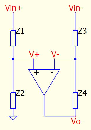
Vo=(Z3Z3+Z4)(Z1+Z2Z2)Vin+−(Z3Z4)Vin−
Now, if to get the same gain as Vin−, we simply set
(Z3Z3+Z4)(Z1+Z2Z2)=(Z3Z4)
Z2Z1+Z2=Z4Z3+Z4
Z2Z1=Z4Z3
Now, we can easily set Z1=Z3 and Z2=Z4 to subtract the signal scaled by Z3Z4
Instrumentation Amplifier
A common amplifier is the instrumentation amplifier or INA. Before we discuss the advantages of an INA, let us look at the circuit and derive the equation for the output.

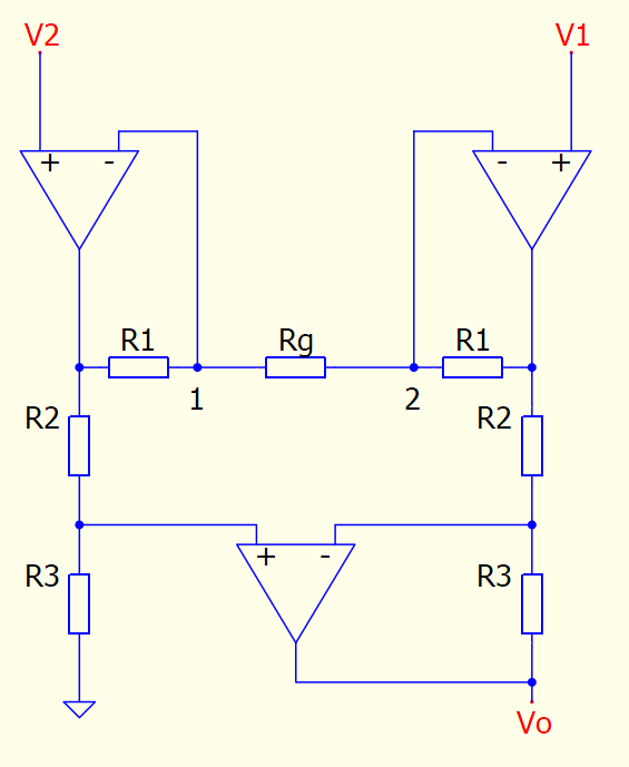
I hope that you can appreciate that the lower half of the circuit is in the same configuration as a difference amplifier, so let us focus on the upper portion.
Looking back at the basic op-amp circuit example, we can say that the output of the left op-amp takes V2 and the voltage at node 2 as inputs, while the right op-amp takes V1 and the voltage at node 1 as inputs.
Thus, the output of the left op-amp is
VL=RgRg+R1V2−RgR1Vn2
and the output of the right op-amp is
VR=RgRg+R1V1−RgR1Vn1
Knowing this, we also know that the final output is
Vo=R2R3[RgRg+R1(V2−V1)−RgR1(Vn2−Vn1)]
Now, note that due to function of the op-amps (makes the non-inverting and inverting inputs equal) and the short from nodes 1 and 2 to the inverting inputs of the op-amp, the following must hold true:
Vn1=V2,Vn2=V1
Therefore,
Vo=R2R3[RgRg+R1(V2−V1)−RgR1(V1−V2)]
=R2R3(RgRg+R1+RgR1)(V2−V1)
=R2R3(1+Rg2R1)(V2−V1)
Finally, we have a gain of
V2−V1Vo=R2R3(1+Rg2R1)
Now the obvious question is, why use an INA when a difference amplifier does the same job? The answer lies within the imperfections and tolerances of real-world components.
Going back to the difference amplifier, let us consider what happens when R1=aR3 and R2=bR4 to account for imbalances in resistor values. Then, returning to this equation
Vo=(R3R3+R4)(R1+R2R2)Vin+−(R3R4)Vin−
We get the following equation with adjusted values
Vo=(R3R3+R4)(aR3+bR4bR4)Vin+−(R3R4)Vin−
=(R3R3+R4)(aR3+bR4bR4)Vin+−(R3R4)Vin−
If we consider VCOM=2Vin++Vin− and Vd=Vin+−Vin− such that Vin+=VCOM+2Vd and Vin+=VCOM−2Vd, then we can rewrite the equation above:
Vo=(R3R3+R4)(aR3+bR4bR4)(VCOM+2Vd)−(R3R4)(VCOM−2Vd)
=VCOM[(R3R3+R4)(aR3+bR4bR4)−(R3R4)]−2Vd[(R3R3+R4)(aR3+bR4bR4)+(R3R4)]
While ideally, we would only see Vd in the output, when the resistors are not perfectly balanced, the common-mode term gets amplified by a factor of
ACOM=G+HG−H
while the difference term gets amplified by a factor of
Ad=H+G(1+H)G+2G2
where G=R3R4 and H=ba.
From this, we can get common-mode rejection ratio, or CMRR, typically expressed in dB.
CMRRdB=20log10(∣AdACOM∣)
Line Level
####
Citations
- Horowitz, P., & Hill, W., (2015) The Art of Electronics
- Self, D. (2010) Small Signal Audio Design